18. Diode
The diode examples are located in the examples/diode. They demonstrate the use of packages located in the python_packages directory to simulate drift-diffusion using the Scharfetter-Gummel method [10].
18.1. 1D diode
18.1.1. Using the python packages
For these examples, python modules are provided to supply the appropriate model and parameter settings. A listing is shown in Table 18.1.
The devsim.python_packages module is part of the distribution. The example files in the DEVSIM distribution set the path properly when loading modules.
|
Creation of models and their derivatives |
|
Ramping bias and automatic stepping |
|
Functions for calculating bulk electron and hole current |
|
Functions for setting up device physics |
For this example, diode_1d.py, the following line is used to import the relevant physics.
from devsim import *
from simple_physics import *
18.1.2. Creating the mesh
This creates a mesh \(10^{-5}\) cm long with a junction located at the midpoint. The name of the device is MyDevice with a single region names MyRegion. The contacts on either end are called top and bot.
def createMesh(device, region):
  create_1d_mesh(mesh="dio")
  add_1d_mesh_line(mesh="dio", pos=0, ps=1e-7, tag="top")
  add_1d_mesh_line(mesh="dio", pos=0.5e-5, ps=1e-9, tag="mid")
  add_1d_mesh_line(mesh="dio", pos=1e-5, ps=1e-7, tag="bot")
  add_1d_contact  (mesh="dio", name="top", tag="top", material="metal")
  add_1d_contact  (mesh="dio", name="bot", tag="bot", material="metal")
  add_1d_region   (mesh="dio", material="Si", region=region, tag1="top", tag2="bot")
  finalize_mesh(mesh="dio")
  create_device(mesh="dio", device=device)

device="MyDevice"
region="MyRegion"

createMesh(device, region)
18.2. Physical Models and Parameters
####
#### Set parameters for 300 K
####
SetSiliconParameters(device, region, 300)
set_parameter(device=device, region=region, name="taun", value=1e-8)
set_parameter(device=device, region=region, name="taup", value=1e-8)

####
#### NetDoping
####
CreateNodeModel(device, region, "Acceptors", "1.0e18*step(0.5e-5-x)")
CreateNodeModel(device, region, "Donors",    "1.0e18*step(x-0.5e-5)")
CreateNodeModel(device, region, "NetDoping", "Donors-Acceptors")
print_node_values(device=device, region=region, name="NetDoping")

####
#### Create Potential, Potential@n0, Potential@n1
####
CreateSolution(device, region, "Potential")

####
#### Create potential only physical models
####
CreateSiliconPotentialOnly(device, region)

####
#### Set up the contacts applying a bias
####
for i in get_contact_list(device=device):
  set_parameter(device=device, name=GetContactBiasName(i), value=0.0)
  CreateSiliconPotentialOnlyContact(device, region, i)


####
#### Initial DC solution
####
solve(type="dc", absolute_error=1.0, relative_error=1e-12, maximum_iterations=30)

####
#### drift diffusion solution variables
####
CreateSolution(device, region, "Electrons")
CreateSolution(device, region, "Holes")

####
#### create initial guess from dc only solution
####
set_node_values(device=device, region=region,
  name="Electrons", init_from="IntrinsicElectrons")
set_node_values(device=device, region=region,
  name="Holes", init_from="IntrinsicHoles")

###
### Set up equations
###
CreateSiliconDriftDiffusion(device, region)
for i in get_contact_list(device=device):
  CreateSiliconDriftDiffusionAtContact(device, region, i)

###
### Drift diffusion simulation at equilibrium
###
solve(type="dc", absolute_error=1e10, relative_error=1e-10, maximum_iterations=30)

####
#### Ramp the bias to 0.5 Volts
####
v = 0.0
while v < 0.51:
  set_parameter(device=device, name=GetContactBiasName("top"), value=v)
  solve(type="dc", absolute_error=1e10, relative_error=1e-10, maximum_iterations=30)
  PrintCurrents(device, "top")
  PrintCurrents(device, "bot")
  v += 0.1

####
#### Write out the result
####
write_devices(file="diode_1d.dat", type="tecplot")
18.2.1. Plotting the result
A plot showing the doping profile and carrier densities are shown in Fig. 18.1. The potential and electric field distribution is shown in Fig. 18.2. The current distributions are shown in Fig. 18.3.
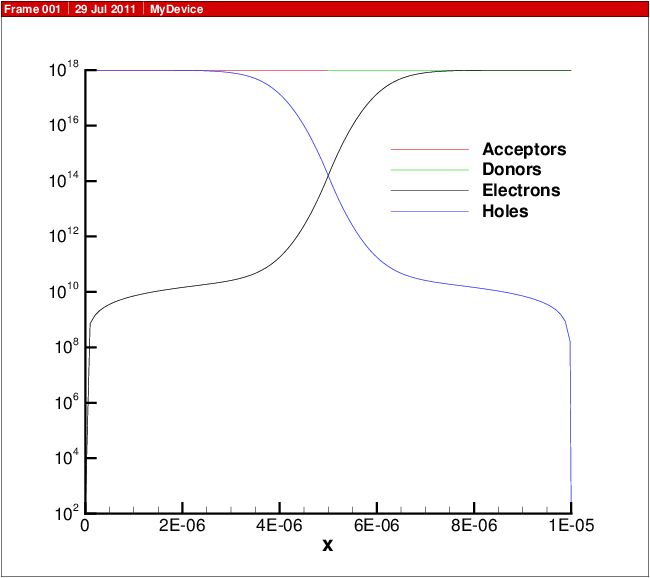
Fig. 18.1 Carrier density versus position in 1D diode.
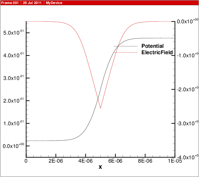
Fig. 18.2 Potential and electric field versus position in 1D diode.
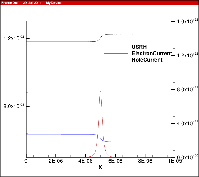
Fig. 18.3 Electron and hole current and recombination.